Gallium Arsenide (GaAs)
Description
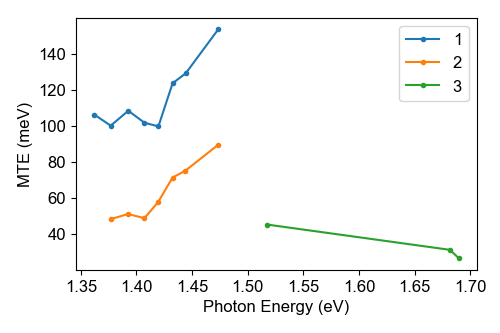
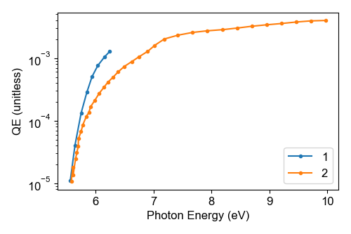
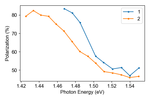
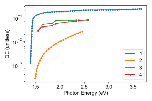
Gallium Arsenide (GaAs) is a III-V semiconductor with a bandgap of 1.4 eV and the ability to achieve negative electron affinity (after activation). These properties make it an attractive choice for a variety of detectors and the production of high-brightness electron beams. GaAs photocathodes are known for their high quantum efficiency and low mean transverse energy. However, they tend to be sensitive to vacuum conditions, which can affect their performance. Negative electron affinity can be achieved through several activation techniques, such as the deposition of a monolayer of Cesium (Cs) on the surface, or through the alternate application of Cs and one of Oxygen (O) or Nitrogen Trifluoride (NF3) commonly referred to as the Yo-Yo activation method.
Photoemission Properties (Cs-NF3)
Photoemission Properties (Clean Surface)
Photoemission Properties (GaAs-GaAsP Superlattice)
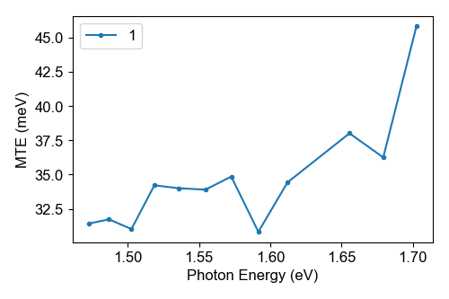
| # | Reference | Save |
|---|---|---|
| 1 | Thermal emittance measurements for electron beams… | ↓ |
Photoemission Properties (Strained)
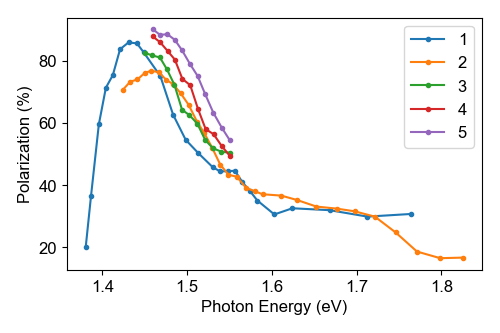

Photoemission Properties (Cs/Cs-O Activation)
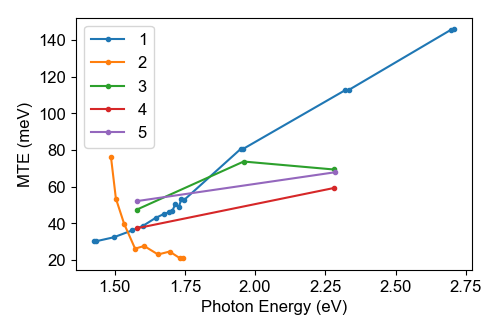
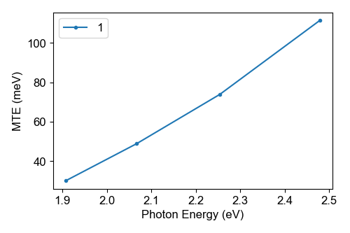
| # | Reference | Save |
|---|---|---|
| 1 | Transverse Energy Distribution Measurements for P… | ↓ |
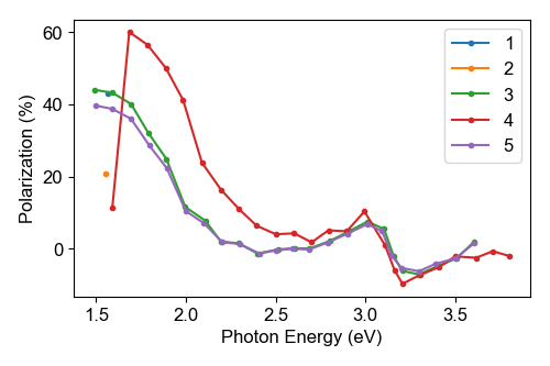
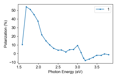
| # | Reference | Save |
|---|---|---|
| 1 | Photoemission of spin-polarized electrons from Ga… | ↓ |
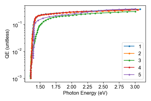
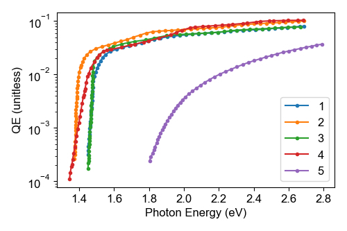
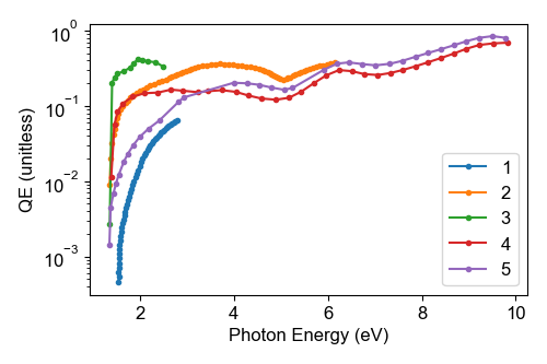
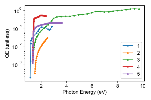
Although best efforts have been made to ensure the accuracy of the data shown on this website, it is provided as-is including any possible errors. We recommend double-checking it against the linked reference(s) before any serious use.
